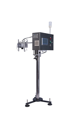
What is Machine Vision?
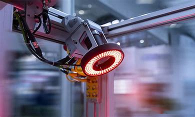
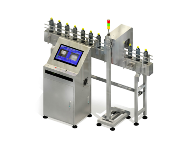
Machine vision uses machines to replace the human eye in measurement and judgment. A machine vision system uses machine vision products (i.e., image capture devices, available in CMOS and CCD) to convert captured objects into image signals. These signals are then transmitted to a dedicated image processing system, which converts them into digital signals based on pixel distribution, brightness, color, and other information. The image system then performs various operations on these signals to extract the target's features and, based on the resulting information, controls the operation of on-site equipment.
Vision System Components:
1. Illumination Source
2. Lens
3. Industrial Camera
4. Image Capture/Processing Card
5. Image Processing System
6. Other External Devices
I. Cameras
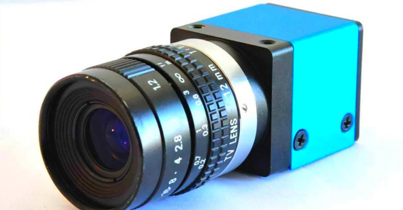
Industrial cameras, also known as video cameras, offer superior image stability, high transmission speed, and high interference immunity compared to traditional consumer cameras. Currently, most industrial cameras on the market are based on CCD (Charge Coupled Device) or CMOS (Complementary Metal Oxide Semiconductor) chips.
Of these, CCD is the most commonly used image sensor in machine vision. It integrates photoelectric conversion, charge storage, charge transfer, and signal readout, making it a typical solid-state imaging device.
The CCD's distinguishing feature is that it uses charge as its signal, unlike other devices that use current or voltage as their signal. This type of imaging device forms charge packets through photoelectric conversion, which are then transferred and amplified by a drive pulse to output the image signal.
A typical CCD camera consists of an optical lens, a timing and synchronization signal generator, a vertical driver, and analog/digital signal processing circuits. As a functional device, the CCD offers advantages over vacuum tubes, such as no burn-in, no lag, low-voltage operation, and low power consumption.
The development of CMOS image sensors first appeared in the early 1970s. With the advancement of very large-scale integrated circuit (VLSI) manufacturing technology in the early 1990s, CMOS image sensors experienced rapid growth.
CMOS image sensors integrate a photosensitive element array, image signal amplifier, signal readout circuitry, analog-to-digital conversion circuitry, image signal processor, and controller on a single chip. They also offer the advantage of programmable random access to local pixels. Currently, CMOS image sensors are widely used in high-resolution and high-speed applications due to their excellent integration, low power consumption, high-speed transmission, and wide dynamic range.
Classification:
Everything has its own classification standards, and industrial cameras are no exception.
Based on chip type, they can be divided into CCD cameras and CMOS cameras;
Based on the structural characteristics of the sensor, they can be divided into line scan cameras and area scan cameras;
Based on the scanning method, they can be divided into interlaced scan cameras and progressive scan cameras;
Based on the resolution, they can be divided into standard resolution cameras and high-resolution cameras;
Based on the output signal method, they can be divided into analog cameras and digital cameras;
Based on the output color, they can be divided into monochrome (black and white) cameras and color cameras;
Based on the output signal speed, they can be divided into standard speed cameras and high-speed cameras;
Based on the response frequency range, they can be divided into visible light (standard) cameras, infrared cameras, and ultraviolet cameras, among others.
Differences:
1. Stable and reliable performance and easy installation. The camera structure is compact and durable, not easily damaged, and has a long continuous operating time and can be used in harsh environments. Ordinary digital cameras cannot achieve this. For example, a consumer digital camera would definitely struggle if it were to operate 24 hours a day or for several days straight.
2. Its shutter speed is very short, allowing it to capture high-speed motion. For example, if you attach a business card to the blades of an electric fan spinning at maximum speed, set a suitable shutter speed, and capture an image with an industrial camera, you'll still be able to clearly discern the font on the card. It's impossible to achieve the same effect with a regular camera.
3. Image sensors use progressive scanning, while regular cameras use interlaced scanning. The production process for progressive scanning image sensors is complex, resulting in low yields and low shipment volumes. Only a few companies worldwide, such as Dalsa and Sony, can offer such products, and they are expensive.
4. Its frame rate is much higher than that of regular cameras. Industrial cameras can capture ten to several hundred frames per second, while regular cameras can only capture two or three frames per second—a significant difference.
5. The output is raw data, often with a wider spectral range, making it suitable for high-quality image processing algorithms, such as those used in machine vision applications. Images captured by ordinary cameras have a spectral range suitable only for human vision and are compressed using MJPEG, resulting in poor image quality and poor analysis and processing.
6. They are more expensive than standard cameras (DSCs).
How to Choose:
1. Choose a CCD or CMOS camera depending on the application. CCD industrial cameras are primarily used for image extraction of moving objects, such as in machine vision for placement machines. However, with the advancement of CMOS technology, many placement machines are also adopting CMOS industrial cameras. CCD industrial cameras are generally used in automated visual inspection solutions or industries. CMOS industrial cameras are increasingly popular due to their low cost and power consumption.
2. When choosing resolution, first consider the accuracy of the object to be observed or measured. Select a resolution based on this accuracy. Camera pixel accuracy = unidirectional field of view / camera unidirectional resolution. Therefore, camera unidirectional resolution = unidirectional field of view / theoretical accuracy. If the field of view is 5mm long and the theoretical accuracy is 0.02mm, then unidirectional resolution = 5 / 0.02 = 250. However, to increase system stability, a single pixel isn't used to correspond to a single measurement/observation accuracy value. Generally, a magnification of 4 or higher is selected. Therefore, the camera requires a single-axis resolution of 1000, so 1.3 million pixels is sufficient.
Next, consider the industrial camera's output. For stereoscopic observation or machine software analysis and recognition, high resolution is helpful. For VGA or USB output, observation on a monitor depends on the monitor's resolution. Even a high-resolution industrial camera is useless if the monitor's resolution is insufficient. High resolution is also helpful for using memory cards or taking photos.
3. Lens Matching: The sensor chip size must be smaller than or equal to the lens size, and the C or CS mount must also be compatible (or an adapter can be added).
4. Camera Frame Rate Selection: When measuring objects with motion, choose an industrial camera with a high frame rate. However, generally speaking, the higher the resolution, the lower the frame rate.
II. Lens
Basic Knowledge:
1. Lens Matching
How do you choose the right lens? When choosing a lens, you need to select one that matches the camera interface and the size of the CCD. Lenses with C and CS mounts are the most common. Small CS-mount cameras for security are gaining popularity, while the FA industry primarily uses C-mount cameras and lens combinations. The corresponding CCD sizes on the market generally range from 2/3-inch to 1/3-inch, depending on the application.
2. Interchangeability
C-mount lenses can be used interchangeably with both C-mount and CS-mount cameras; CS-mount lenses cannot be used with C-mount cameras, only with CS-mount cameras.
3. KERARE
When a camera uses a lens with a small CCD, the surrounding areas not captured by the image appear black, a condition known as kerare.
4. Function of the Lens:
Lens design involves grinding various materials with different refractive indices into high-precision curved surfaces and combining these materials. Its basic principle is a common technique used since the time of Galileo. To achieve even clearer images, new materials and aspherical lenses are being researched and developed.
3. Light Sources
LED light sources, halogen lamps (fiber optic light sources), and high-frequency fluorescent lamps. LED light sources are currently the most commonly used, offering the following key features:
They can be manufactured in various shapes, sizes, and illumination angles;
They can be manufactured in various colors as needed, and the brightness can be adjusted at any time;
The heat dissipation device provides improved heat dissipation and more stable brightness;
They have a long service life;
They respond quickly, reaching maximum brightness in 10 microseconds or less;
The power supply features an external trigger, allowing computer control, fast startup, and can be used as a strobe light;
LEDs offer low operating costs and long life, offering significant advantages in terms of overall cost and performance;
Custom designs can be tailored to customer needs.
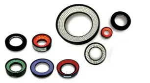
LED light sources can generally be categorized by shape:
1. Ring Light Sources: Ring light sources offer different illumination angles and color combinations, enhancing the three-dimensional details of objects. They also feature high-density LED arrays for high brightness, a variety of compact designs, and space-saving installation. They also address diagonal shadowing issues. Optional diffusers provide even light distribution. Applications include PCB substrate inspection, IC component inspection, microscope illumination, LCD calibration, plastic container inspection, and integrated circuit printing inspection. 2. The backlight utilizes a high-density LED array to provide high-intensity backlighting, highlighting the object's contours and features, making it particularly suitable for use as a microscope stage. Dual-use red and white backlights, as well as multi-use red and blue backlights, can be configured to produce different colors to meet the multi-color requirements of different test objects. Applications include: dimensional measurement of mechanical parts, appearance inspection of electronic components and ICs, film stain detection, and scratch detection of transparent objects.
3. Bar Light Source: Bar light sources are the preferred light source for larger square structures. Colors can be freely combined and matched to meet specific requirements, and the illumination angle and mounting are adjustable. Applications include: metal surface inspection, image scanning, surface crack detection, and LCD panel inspection.
4. Coaxial Light Source: Coaxial light sources eliminate shadows caused by surface unevenness, thereby reducing interference. Some utilize a beam splitter design to minimize light loss, improve image clarity, and provide uniform illumination of the surface. Applications: This series of light sources is ideal for scratch inspection on highly reflective surfaces such as metal, glass, film, and wafers; chip and silicon wafer breakage detection; mark location; and package barcode recognition.
5. AOI-specific light source: Three-color illumination at different angles highlights the three-dimensional information of solder. A diffuser guides the light to reduce reflections. Different angle combinations are available. Applications: Used for solder inspection on circuit boards.
6. Spherical integrating light source: The inner surface of a hemispherical sphere with an integrating effect evenly reflects light emitted from the bottom 360 degrees, ensuring uniform illumination across the entire image. Applications: Suitable for inspecting curved, uneven, and curved surfaces, as well as highly reflective metal and glass surfaces.
7. Linear light source: Ultra-high brightness, using a cylindrical lens to focus the light, making it suitable for continuous inspection in various assembly lines. Applications: Dedicated for array camera illumination and AOI. 8. High-power LED point light source, compact size, and high luminous intensity. It's an alternative to fiber-optic halogen lamps, particularly suitable as a coaxial light source for lenses. Its efficient heat dissipation significantly extends the light source's lifespan. Applications: Suitable for use with telecentric lenses, chip inspection, mark location, and wafer and LCD glass substrate alignment.
9. Combined Bar Light Source: Four-sided bar light distribution, each with independent controllable illumination. The required illumination angle can be adjusted to suit the object under test, offering a wide range of applications. Applications include CB substrate inspection, IC component inspection, solder inspection, mark location, microscope illumination, package barcode illumination, and spherical object illumination.
10. Alignment Light Source: Fast alignment, wide field of view, high precision, compact size for easy inspection and integration, high brightness, and an optional auxiliary ring light source. Applications: The VA series light source is specifically designed for alignment in fully automatic circuit board printers. 4. Selection of light source
1. Prerequisite information
(1) Inspection content: Appearance inspection, OCR, dimension measurement, positioning
(2) Object
What do you want to see? (Foreign matter, scratches, defects, marks, shapes, etc.)
Surface condition (mirror, rough surface, curved surface, flat surface)
Three-dimensional? Flat surface?
Material, surface color
Field of view?
Dynamic or static (camera shutter speed)
(3) Restrictions
Working distance (distance from the bottom of the lens to the surface of the object being measured)
Setting conditions (lighting size, distance from the bottom of the lighting to the surface of the object being measured, reflective or transmissive)
Ambient environment (temperature, external stray light)
Camera type: area array or linear array
2. Simple preliminary knowledge:
(1) Due to different materials and thicknesses, the light transmission characteristics (transparency) vary. (2) The ability of light to penetrate materials (transmittance) varies according to the length of its wavelength. (3) The longer the wavelength of light, the stronger its ability to penetrate the material. The shorter the wavelength of light, the greater its diffusion rate on the surface of the material. (4) Transmitted illumination is a method of transmitting light through the object and observing the transmitted light.
3. Light source:
A stable and uniform light source is extremely important
Purpose: To distinguish the object under test from the background as clearly as possible
When capturing an image, the most important thing is how to clearly obtain: the difference in light and dark between the object under test and the background
Currently, the most widely used technical method in the field of image processing is: binarization (white and black) processing. In order to highlight feature points and feature images, the commonly used lighting methods include bright field and dark field.
Bright field: Use direct light to observe the entire object (scattered light appears black)
Dark field: Use scattered light to observe the entire object (direct light appears white) The specific method of light source selection still depends on practical experience in the experiment.

